![]()
![]()
![]()
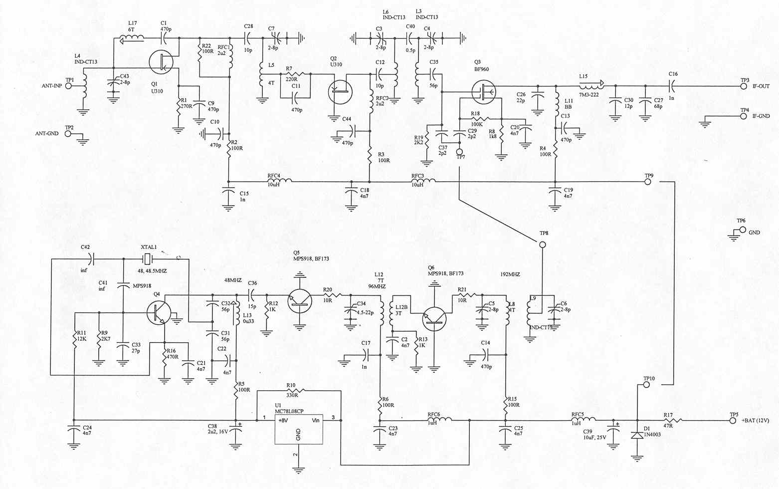
222-224MHz to 28-30Mhz Low Noise
JFET-Converter
by VE6AQO
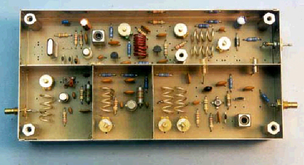
Below is some information about the design of my 220MHZ to 10M Converter. The goal was to obtain best possible performance with off-the-shelf commonly available parts. Acceptable adjustment must be possible without expensive test equipment. SMD-parts were intentionally avoided due to the difficulties in procurement and minimum quantities often imposed. The 310 series FETS are readily available and cheap. Dual gate MOS-FETS such as BF982 and similar are only available as SMD parts. Instead a cascode type circuit was chosen. No effort was made to breed a converter for EME or other extreme type of operation. It provides good, but not outstanding performance for normal Amateur work. With the receiver in SSB mode, signals as low as 0.05uV were reliably received (MB103 Semco Receiver Board). Another goal was to be able to use a single sided printed circuit board to simplify etching the board.
|
 |
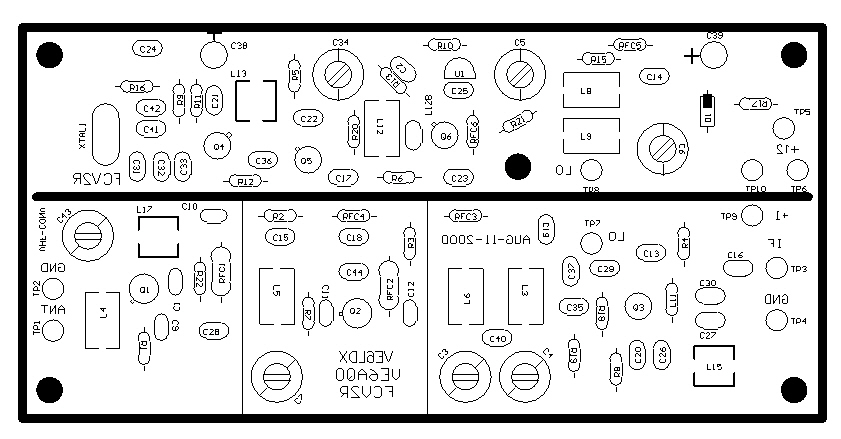 |
 (Mirror Bottom View) |
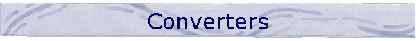
Please click on thumbnails to view pictures.
Some construction notes:
Some important coil data will be added later. Some information is given below.
The There are two versions of photo positive masks. For best results use the mirror version to ensure the photo emulsion or toner faces the photo resist during exposure.
Some options must be set correctly and will be described later.
A German made tinned steel enclosure was used, but is not necessary.
Silver plated wire (0.8-1mm) is used for the VHF coils. Tinned wire will degrade performance. If not available, use enamelled wire (AWG#20 or ca. 0.8-1mm diameter.
L15 is made by Coilcraft, part number 7M3-222.
L3 Tap is 1T from ground side. (The picture shows higher tap point)
L4 tap is about 1.5T from ground side.
If no sweeper is available, tune L4, L5 for maximum, L6 at 220MHz for maximum, L3 at 225MHz. This technique will actually result in a nice flat top symmetrical response. The neutralisation coil, L17 should be tuned for minimum gain. A noticeable drop in noise should be audible. It must resonate at 223MHz. Improper adjustment will result in instability of Q1 and poor performance.
2N4416 can be substituted for J/U310.
MPS918, 2N708 or other similar transistors can be substituted for Q4, Q5, and Q6. Even 2N3904 work reasonably well.
The response is flat from 221 to 224 MHz for -3dB.
Converter gain was measured to be 22dB at 223MHz.
Image rejection was measured to be better then 96dB at 168Mhz.
Spurious receptions: Although two high power television stations operating in the vicinity of 220MHz are located in Edmonton, no adverse effects can be noted. The only spurious signals found, come from leakage of the nearby cable-TV system, resulting in a weak carrier around 223MHz. So far no intermodulation interference was noticed. The 220MHz Band is totally free from adjacent telecommunication services that plague the 2-m Band nowadays. This makes it possible to get good results with simple equipment.
The mixer output circuit was implemented as a low-pass filter impedance transformation network. It is simple to tune and exhibits the required power bandwidth.
Capacitors C41 and C42 are actually intended as jumper selection holes. C41 has a jumper wire placed to complete the crystal circuit to the base of Q4.
Mixer Injection: Two methods of coupling the 116MHz energy are provided. For experimentation, the L.O. signal can either be applied to the base or the source of Q3. In this version, only C37 is used to add the L.O. signal to the mixer gate number one.
Converter Crystal should be 48MHz for an IF range of 28-30MHz and 220-222MHz.
For 222-224 the crystal frequency should be 48.5MHz. (third overtone crystal). My crystal was custom manufactured by ICM.
Noise Figure wasn't measured yet, but should be around 2.5-3dB. Noise source based optimization is required for optimum results.
The board size is approximately 5.765x2.820 inches. The odd dimensions of the circuit board were imposed by the enclosure the board was soldered into. The shielded enclosure is optional to prevent external pickup of signals by the components.
The photo mask provided should be printed out on clear presentation film on a laser or inkjet printer. The scale is 1:1. For best sharpness make sure the toner or ink side faces the photo resist. This is why the mask is shown as a mirror image.
PDF drawings and with all drawings can be downloaded here - FCV2.ZIP (About 907KB)
Please wait for a future article properly describing the converter and its adjustments. The original board was not etched but mechanically engraved using a CNC circuit board milling machine.
© Copyright 2002-2010 VE6AQO & DL9BBR